User Tools
Sidebar
Table of Contents
This is an old revision of the document!
Etching PCBs
Disclaimer
This instruction has been written for a supervised session performed in a chemical lab. Be careful when applying to a different environment.
Introduction
This instruction is about producing printed circuit boards (PCBs) from already prepared designs. There are two major techniques for PCB manufacturing. For prototyping purposes it is popular to use a special milling machine for PCBs. The faculty uses a LPKF ProtoMat S62 in its electrical workshop. EAGLE board designs are exported to gerber and excellon files and after making some adjustments in a CAM tool like CircuitCAM designs can be used for milling out copper-clad boards. The machine isolates all traces on the board and drills holes where necessary.
The technique which is covered here employs a chemical process to create PCBs. To put it simply it is a four step procedure:
- prepare development and etching solutions
- expose board to uv light while protecting certain areas with a mask
- develop board using sodium hydroxide
- etch board using sodium persulfate
The industry also these principle steps for mass production of PCBs.
Resources
The design should already be finished and a mask for uv exposure
Magnetrührer, Waage, Spatel, Glasrührstab, Becherglas 2l, 500ml, Becherglas für 300g, Thermometer, Ethanol, Papiertücher, Torx-Schraubendreher, Tacker, Scheren ruler, scissors, plate shear, chemistry lab, sink, fume extractor, safety goggles, lab coat, gloves, printer, transparent foil, uv exposer devices, fotosensitive base material, development and etching solution, containers, etching bath, aceton, Wattepads, Lötlack
Safety instructions
Please read the chemistry lab safety rules on Moodle before taking the experiment. The safety rules will also be pointed out at the beginning of the experiment.
We will work with the following substances in this lab:
- toner compressor
- Developer / sodium hydroxide (Natriumhydroxid, NaOH)
- Etchant / sodium persulafte (Natriumpersulfat, Na2S2O8)
- item ethanol (C2H6O)
- item distilled (purified) water (H2O)
Set up developing and etching solutions
Get your safety equipment. This includes glasses, lab coat and gloves. Make yourself familiar with the provided tools.
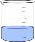
- Fill the beaker with 250 ml distilled water.
- Get 5g sodium hydroxide from the front of the classroom and fill it into your beaker. In order to get the right amount use the precision scale and a weighing boat. Close the container of sodium hydroxide as sodium hydroxide is hrydrophilic.
- Stir the liquid in the beaker with a glass rod until everything is dissolved.
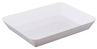
- Pour the solution into the plastic bowl.
- Fill the big beaker with approximately 1.6 liter of distilled water.
- Add 300g sodium persulfate to it, it should be already prepared in the second beaker.
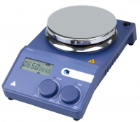
- Use the magnetic stirrer to heat the big beaker up and help dissolving the sodium persulfate at the same time (setting 4 / 4). As etching etching works best above 40°C (and below 50°C). Try to heat the solution up until it reaches 40°C.
- When the solution is ready turn off the magnetic stirrer and pour the solution carefully into the etching device.
- Turn on the heating and air compressor of the etching device by plugging it into the electric outlets.
UV exposure
- Get the transparent foils containing your PCB design.
- Go to the fume cupboard at the end of the room and apply some density spray to both foils. Make sure to apply it on the side with the printing.
- Wait for it to dry. The black areas should be clearly darker now.
- Use the scissors to cut out your design. Leave a big surrounding area, as you will nedd it for stapeling.
- Place the foils on top of each other. The sides with the printing on it have to be facing each other (the board will be in between of the foils later).
- Staple the foils together while trying to align them perfectly.
- Check the alignment. Misalignments will probably result in defective PCBs later.
- Get a piece of fotensensitive base material (FR4 in this case) for exposure. It will be slightly bigger than your design so you should have no problems with that.
- Remove the blue protection foil (see figure 4) on both sides.
- Avoid exposing the unprotected plate to sunlight (all UV sources).
- Beware: For your own safety avoid looking into the uv lights. The device is to be only turned on when closed!
- Turn it on and wait for the vacuum to go up to 0.3, compare to figure 7. The vacuum prevents things from moving.
- Set the exposure time to two minutes and thirty seconds (the display should read 2-3-0), make sure the bottom lights are also enabled as you are making a two sided PCB and start the device by pressing the knob once.
- When the time is up the lights will automatically be turned off and the vacuum will be released.
- Open the device and get out the exposed board.
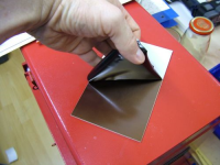 Fig. 4: Remove protection foil
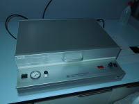 Fig. 5: UV exposure device
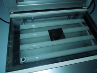 Fig. 6: Board under plate
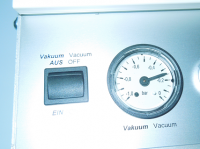 Fig. 7: Check vacuum
Developing and etching the board
- Remove the exposed board from the foils.
- Put the board into the prepared bowl of the development solution. Stir it with a stick.
- Brown residues from the exposed parts of the board should start to appear after a couple of seconds. Stir until the process seems to stop and take it out immediately. Do not leave the board in for longer than 90 seconds maximum.
- Rinse the board thoroughly with (purified) water.
- Check the temperature of the etching solution, it should be above 40 and below 50 degrees C.
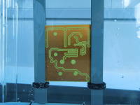
- Mount the board to the grey retainer (see figure 8). To speed up the procution process mount two boards at the same time.
- Submerge the board(s) in the tank.
- Wait for the etching process to complete. You may have to wait a couple of minutes before something seems to be happening but from this point it should be going quite fast and obvious.
- Take out the board when etching is complete. Do not wait to long as it will affect the protected traces as well if you wait too long.
- Rinse the board(s) thoroughly with (purified) water.
- Repeat these steps until all team members have a PCB.
- Shut down pump and heating.
- Use ethanol and paper tissue to remove the remaining photoresist from the board(s). Be thorough.
- Let the board(s) dry.
- Clean the lab equipment, rinse everything with water.
- Dispose of waste properly.

